標題: Titlebook: Radio-Frequency Microelectronic Circuits for Telecommunication Applications; Yannis E. Papananos Book 1999 Springer-Verlag US 1999 CMOS.co [打印本頁] 作者: miserly 時間: 2025-3-21 19:02
書目名稱Radio-Frequency Microelectronic Circuits for Telecommunication Applications影響因子(影響力)
書目名稱Radio-Frequency Microelectronic Circuits for Telecommunication Applications影響因子(影響力)學科排名
書目名稱Radio-Frequency Microelectronic Circuits for Telecommunication Applications網(wǎng)絡公開度
書目名稱Radio-Frequency Microelectronic Circuits for Telecommunication Applications網(wǎng)絡公開度學科排名
書目名稱Radio-Frequency Microelectronic Circuits for Telecommunication Applications被引頻次
書目名稱Radio-Frequency Microelectronic Circuits for Telecommunication Applications被引頻次學科排名
書目名稱Radio-Frequency Microelectronic Circuits for Telecommunication Applications年度引用
書目名稱Radio-Frequency Microelectronic Circuits for Telecommunication Applications年度引用學科排名
書目名稱Radio-Frequency Microelectronic Circuits for Telecommunication Applications讀者反饋
書目名稱Radio-Frequency Microelectronic Circuits for Telecommunication Applications讀者反饋學科排名
作者: Stress 時間: 2025-3-21 23:52
Radio-Frequency Microelectronic Circuits for Telecommunication Applications978-1-4757-3017-3作者: infringe 時間: 2025-3-22 03:47
Integrated Passive Elements and Their Usage at High Frequencies,integrated inductors over silicon substrates, along with a CAD tool, have been presented [5,6]. This effort will significantly boost the usage of inductors in silicon integrated circuits, something that has been very common and for many years in . technologies.作者: conjunctiva 時間: 2025-3-22 04:57 作者: Cholecystokinin 時間: 2025-3-22 11:46
anintegrated RF front-end, namely, the LNA, the mixer, the VCO andintegrated filters. Design paradigms are provided classified on thetechnology used in each case: pure bipolar, CMOS, BiCMOS or SiGe...Radio-Frequency Microelectronic Circuits for TelecommunicationApplications. is essential reading for all resea978-1-4419-5104-5978-1-4757-3017-3作者: lesion 時間: 2025-3-22 15:01 作者: 改革運動 時間: 2025-3-22 19:57
Yannis E. Papananoshanging the states of PIN diode switches, an antenna can be made reconfigurable. The substrate used is FR4 having 1.6?mm thickness and a 4.4 dielectric constant. This antenna is analyzed using HFSS 15.0 simulation software. The proposed structure can produce all three reconfiguration properties.作者: Costume 時間: 2025-3-22 23:37
Yannis E. Papananos4?GHz, 9.6%) within 3rd IB. The simulated peak gain between 2.2 and 6.01dBi span throughout IBW region makes the dual CP bands appropriate for some part of S- and X-band, particularly fixed-satellite service (FSS) and synthetic aperture radar (SAR) applications.作者: Epithelium 時間: 2025-3-23 02:22 作者: 無情 時間: 2025-3-23 05:53 作者: 同位素 時間: 2025-3-23 10:53 作者: 信條 時間: 2025-3-23 17:40
Yannis E. Papananoss of diameter ranging from 42.44?μm to 83.30?μm, and pore depth of 49.00?μm to 98.90?μm have been synthesized. Pore size and depth modulation were observed with variation in the power of Pulsed Fiber Laser. The change in the output power of Pulsed Fiber Laser gives a linear relation with pore diamet作者: cardiovascular 時間: 2025-3-23 21:24 作者: 亞麻制品 時間: 2025-3-24 02:06 作者: faction 時間: 2025-3-24 05:46 作者: 歡騰 時間: 2025-3-24 09:59
http://image.papertrans.cn/r/image/820662.jpg作者: ARIA 時間: 2025-3-24 12:44
https://doi.org/10.1007/978-1-4757-3017-3CMOS; communication; electronic circuit; electronics; integrated circuit; modeling; transistor作者: Mumble 時間: 2025-3-24 17:53 作者: 意見一致 時間: 2025-3-24 21:40
Oscillators,The frequency synthesizer is one of the most fundamental cells in a telecommunications transceiver. Its role is to produce the necessary periodic signals for frequency up-conversion in the transmitter and down-conversion in the receiver. The location of the frequency synthesizer in a typical transceiver is depicted in the schematic of Fig. 7.1.作者: 維持 時間: 2025-3-25 00:19
Yannis E. Papananosng system requirements or environmental conditions. Reconfigurability is a factor that changes the characteristics of a particular antenna for obtaining additional functionalities for any system. These antennas are low profile and low priced resulting in a good performance. Moreover, one single ante作者: fibula 時間: 2025-3-25 07:06 作者: 昏暗 時間: 2025-3-25 10:24
Yannis E. Papananosign antenna which is proposed here involves two L-shaped radiators with two asymmetric cross slots within it creating mutual coupling to attain dual circularly polarized (CP) bands. To generate quad impedance bandwidth (IBW), defective ground plane is utilized on the bottom portion on the substrate.作者: 劇毒 時間: 2025-3-25 15:40
Yannis E. Papananosology, power consuming, expensive, and bulky triple modular redundancy and shielding techniques are required to address radiation related issues. In this work, we simulate Semi-Conductor Laboratory (SCL) 180?nm silicon on insulator (SOI) and Bulk NMOS device for comparative study of TID effects in s作者: fulcrum 時間: 2025-3-25 17:22
Yannis E. Papananosn detection. Target tracking is well examined and demanding application of WSNs. Such application needs accurate estimate of a target’s changing spot which composes position and velocity or/and defined measure of distance of target from each sensing nodes. These measures are treated as prerequisites作者: 變形詞 時間: 2025-3-25 22:18
Yannis E. Papananos techniques like metal-assisted etching, layer-by-layer lithographic methods, Reactive Ion Etching (RIE), Inductive Coupled Plasma (ICP), and direct laser writing technique. These techniques have their advantages as well as disadvantages. Among them, Laser etching is a promising option for porous si作者: 殺子女者 時間: 2025-3-26 03:06 作者: 重疊 時間: 2025-3-26 04:21 作者: 表被動 時間: 2025-3-26 09:13
contacts between devices and a huge volume of data. On the other hand, there are many security challenges to protect this information from risk exposure. It’s crucial to note that these devices are compact and use very little power. As a consequence, using several rounds of data encryption would be作者: Myosin 時間: 2025-3-26 12:50 作者: 救護車 時間: 2025-3-26 17:41 作者: faculty 時間: 2025-3-27 00:48 作者: FATAL 時間: 2025-3-27 02:38
The MOS Transistor at High Frequencies,f each stage. Evidently, this practice dramatically increases the system cost but it is a one way solution in many cases. However, at the low end of the frequency band (800 to 2400 MHz), it is now feasible to implement the complete system using Si-based technologies. This fact, drastically reduces t作者: MAPLE 時間: 2025-3-27 07:22
Integrated Passive Elements and Their Usage at High Frequencies,tors, capacitors, resistors). For example, the existence of high quality capacitors and inductors significantly determines the circuit performance and usually their shortage in an IC technology prevents the design of high frequency systems. Capacitors and ohmic resistors are elements that can be eas作者: LAVA 時間: 2025-3-27 13:31
Basic Definitions and Terminology,On the other hand, the microwave telecom system designers are using different methodology and tools (i.e. Smith chart), that help them proceed with their designs in an effective and proper way. The RF IC designer (especially if he comes from the low-frequency integrated circuit design field), must b作者: 仇恨 時間: 2025-3-27 14:07 作者: CON 時間: 2025-3-27 17:45 作者: 語源學 時間: 2025-3-27 23:59 作者: 高調(diào) 時間: 2025-3-28 02:58
Mixers,nals at its inputs (it does not add them linearly) but it multiplies them in pairs. Performing the task of driving the desired signal to the . stage, out of a host of possible combinations of signals appearing at the antenna, is largely a matter of proper system design.作者: rods366 時間: 2025-3-28 06:23
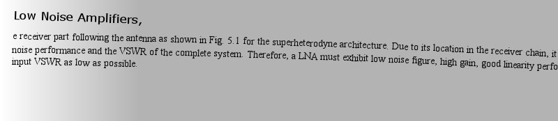
Integrated RF Filters,r circuits in the system, as will be shown later on. The main reasons that keep certain filters out of the chip include the high frequency of operation, the high required quality factor and the stringent specifications in terms of dynamic range and power dissipation. In Fig. 8.1, the receiver part of a super-heterodyne system is shown.作者: agitate 時間: 2025-3-28 11:18
The Bipolar Transistor at High Frequencies,communications receiver, is the RF front-end. Additionally, it is the part of the system that exhibits the highest power consumption. For this purpose, the selection of the proper technology for the integration of this particular subsystem plays a very important role. Among silicon processes, the bipolar technologies are the preferred ones.作者: reptile 時間: 2025-3-28 15:35
The MOS Transistor at High Frequencies,d simultaneously, exhibits the highest level of integration. This solution is investigated in research projects from the Academia but the Industry still remains reluctant in adopting it mainly due to the fact that the MOS transistor exhibits poorer performance than its bipolar counterpart, especially at high frequencies of operation.作者: 吹牛大王 時間: 2025-3-28 19:20
Basic Definitions and Terminology,or this purpose, in the present chapter, the basic definitions and terminology employed in telecommunications systems design will be briefly reviewed. Please note that the definition of phase noise will be postponed until Chapter 7 where the oscillator circuits are presented.