標(biāo)題: Titlebook: Electrical Characterization of Silicon-on-Insulator Materials and Devices; Sorin Cristoloveanu,Sheng S. Li Book 1995 Springer Science+Busi [打印本頁] 作者: Gratification 時間: 2025-3-21 17:17
書目名稱Electrical Characterization of Silicon-on-Insulator Materials and Devices影響因子(影響力)
書目名稱Electrical Characterization of Silicon-on-Insulator Materials and Devices影響因子(影響力)學(xué)科排名
書目名稱Electrical Characterization of Silicon-on-Insulator Materials and Devices網(wǎng)絡(luò)公開度
書目名稱Electrical Characterization of Silicon-on-Insulator Materials and Devices網(wǎng)絡(luò)公開度學(xué)科排名
書目名稱Electrical Characterization of Silicon-on-Insulator Materials and Devices被引頻次
書目名稱Electrical Characterization of Silicon-on-Insulator Materials and Devices被引頻次學(xué)科排名
書目名稱Electrical Characterization of Silicon-on-Insulator Materials and Devices年度引用
書目名稱Electrical Characterization of Silicon-on-Insulator Materials and Devices年度引用學(xué)科排名
書目名稱Electrical Characterization of Silicon-on-Insulator Materials and Devices讀者反饋
書目名稱Electrical Characterization of Silicon-on-Insulator Materials and Devices讀者反饋學(xué)科排名
作者: AV-node 時間: 2025-3-21 22:41
Grundlagen der anorganischen Chemieonductor layer from the semiconductor substrate (i.e., the SIS structure). Methods of forming SIS structures include Separation by IM-plantation of OXygen (SIMOX), Zone-Melting Recrystallization (ZMR) of polysilicon, Epitaxial Lateral Overgrowth (ELO), Full Isolation by Porous Oxidized Silicon (FIPOS), and Wafer Bonding (WB).作者: 致詞 時間: 2025-3-22 02:48
Grundlagen der betrieblichen Personalpolitik. In response to intrinsic problems (large values of the sheet resistance, full depletion, in-depth inhomogeneity, etc.) and new opportunities (substrate bias influence), more refined experimental setup and modeling are necessary.作者: 泛濫 時間: 2025-3-22 06:48 作者: Conduit 時間: 2025-3-22 11:17 作者: superfluous 時間: 2025-3-22 16:40
https://doi.org/10.1007/978-3-322-85672-2-hardened CMOS circuits, the advanced CMOS ULSI, high/low voltage, high temperature devices, three-dimensional circuits, and sensors. Some innovative and speculative components will be presented in the last section.作者: superfluous 時間: 2025-3-22 20:38 作者: 閑聊 時間: 2025-3-23 01:04
Introduction,con technology is now facing very fundamental limitations. At this point, the potential of SOI technologies has become very attractive. SOI devices are more tolerant to the constraints of scaling-down rules, and they perform superbly.作者: Prosaic 時間: 2025-3-23 03:28 作者: Mutter 時間: 2025-3-23 08:57 作者: Endemic 時間: 2025-3-23 10:21 作者: eustachian-tube 時間: 2025-3-23 16:47 作者: 下船 時間: 2025-3-23 21:04
Methods of Forming SOI Wafers,onductor layer from the semiconductor substrate (i.e., the SIS structure). Methods of forming SIS structures include Separation by IM-plantation of OXygen (SIMOX), Zone-Melting Recrystallization (ZMR) of polysilicon, Epitaxial Lateral Overgrowth (ELO), Full Isolation by Porous Oxidized Silicon (FIPOS), and Wafer Bonding (WB).作者: 不持續(xù)就爆 時間: 2025-3-24 00:02 作者: 組裝 時間: 2025-3-24 02:33
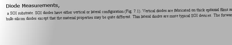
Diode Measurements,ave like bulk-silicon diodes except that the material properties may be quite different. Thin lateral diodes are more typical SOI devices. The forward-and reverse-biased I—V characteristics of a p—n diode make it possible to determine the quality of silicon film, buried-oxide, and interface properties of the SOI material.作者: 先鋒派 時間: 2025-3-24 09:46 作者: obscurity 時間: 2025-3-24 11:25
Grundlagen der anorganischen Chemiecon technology is now facing very fundamental limitations. At this point, the potential of SOI technologies has become very attractive. SOI devices are more tolerant to the constraints of scaling-down rules, and they perform superbly.作者: Dysplasia 時間: 2025-3-24 14:55
Grundlagen der betrieblichen Lohnfindungof the VLSI circuits. Therefore, it is essential that diagnostic tools, including both destructive and nondestructive techniques, be available for the initial assessment of the key physical and electrical parameters of the starting SOI materials.作者: 詞匯 時間: 2025-3-24 21:10
https://doi.org/10.1007/978-3-8348-9927-9ency, high-frequency, and combined high-low-frequency measurements. Two variants of the transient capacitance techniques are examined: the bias-scan and temperature-scan deep-level-transient spectroscopy (DLTS).作者: Habituate 時間: 2025-3-25 01:54
Grundlagen der doppelten Buchführungion, to SOI transistors, provided that they have a contact with the Si film (five-terminal devices) and are fabricated in non-fully depleted films (relatively thick or highly doped). Although the back gate-bias acts as an extra experimental parameter, its practical influence on the operation of partially depleted MOSFETs is rather limited.作者: 大雨 時間: 2025-3-25 03:24 作者: CLAP 時間: 2025-3-25 07:34
The Springer International Series in Engineering and Computer Sciencehttp://image.papertrans.cn/e/image/305702.jpg作者: 堅毅 時間: 2025-3-25 15:12 作者: SEMI 時間: 2025-3-25 19:48 作者: emission 時間: 2025-3-25 23:03 作者: Cabg318 時間: 2025-3-26 03:10
Grundlagen der betrieblichen Lohnfindungd buried oxide, and other electrical and physical properties (carrier lifetime, interface trapping, etc.) of the starting wafers prior to the fabrication of SOI devices and circuits. Fluctuations in quality and uniformity of SOI materials have great impact on the performance, yield, and reliability 作者: 賞心悅目 時間: 2025-3-26 05:05 作者: overture 時間: 2025-3-26 08:48
https://doi.org/10.1007/978-3-8348-9927-9aces and in the buried oxide of the SOI material by using its inherent silicon—insulator—silicon (SIS) capacitor structure. The techniques include small-signal a.c. capacitance and conductance as well as transient capacitance methods.[.,.] The capacitance and conductance methods consist of low-frequ作者: Factorable 時間: 2025-3-26 12:56
Verkettete Codes und iterative Decodierung a SOI substrate. SOI diodes have either vertical or lateral configuration (Fig. 7.1). Vertical diodes are fabricated on thick epitaxial films and behave like bulk-silicon diodes except that the material properties may be quite different. Thin lateral diodes are more typical SOI devices. The forward作者: 大喘氣 時間: 2025-3-26 17:26 作者: CROW 時間: 2025-3-26 21:01 作者: 菊花 時間: 2025-3-27 01:58 作者: expansive 時間: 2025-3-27 07:03 作者: Magnificent 時間: 2025-3-27 11:06 作者: 熒光 時間: 2025-3-27 14:00
Grundlagen der doppelten Buchführung properties of SOI materials. Even after complete processing of integrated circuits, the interface quality and some of the crystalline imperfections of the incipient SOI wafer are still transparent in transistor characteristics.作者: Adj異類的 時間: 2025-3-27 19:10
Transistor-Based Characterization Techniques, properties of SOI materials. Even after complete processing of integrated circuits, the interface quality and some of the crystalline imperfections of the incipient SOI wafer are still transparent in transistor characteristics.作者: precede 時間: 2025-3-27 23:50 作者: Inveterate 時間: 2025-3-28 05:14 作者: DIKE 時間: 2025-3-28 09:43 作者: 先行 時間: 2025-3-28 14:03 作者: Default 時間: 2025-3-28 15:13
Methods of Forming SOI Wafers,he case for silicon on sapphire (SOS) and silicon on zirconia (SOZ). In the second group, a thin insulating layer is used to separate the active semiconductor layer from the semiconductor substrate (i.e., the SIS structure). Methods of forming SIS structures include Separation by IM-plantation of OX作者: 金絲雀 時間: 2025-3-28 21:30 作者: facilitate 時間: 2025-3-28 23:59
Wafer-Screening Techniques,d buried oxide, and other electrical and physical properties (carrier lifetime, interface trapping, etc.) of the starting wafers prior to the fabrication of SOI devices and circuits. Fluctuations in quality and uniformity of SOI materials have great impact on the performance, yield, and reliability 作者: MUTE 時間: 2025-3-29 07:08 作者: absolve 時間: 2025-3-29 10:09
SIS Capacitor-Based Characterization Techniques,aces and in the buried oxide of the SOI material by using its inherent silicon—insulator—silicon (SIS) capacitor structure. The techniques include small-signal a.c. capacitance and conductance as well as transient capacitance methods.[.,.] The capacitance and conductance methods consist of low-frequ作者: 四目在模仿 時間: 2025-3-29 13:14