作者: 脫水 時間: 2025-3-21 22:40
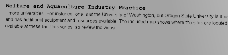
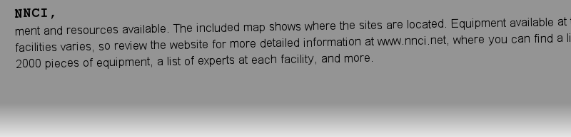
NNCI,r more universities. For instance, one is at the University of Washington, but Oregon State University is a partner institute and has additional equipment and resources available. The included map shows where the sites are located. Equipment available at these facilities varies, so review the websit作者: Euthyroid 時間: 2025-3-22 03:49 作者: 武器 時間: 2025-3-22 06:27
MEMS Fabrication Process, the graphic that illustrates this basic process. You start with a silicon wafer and apply a photosensitive coating to it that is called photoresist. When you expose your coated wafer to UV light, the regions blocked by your glass mask (containing your pattern for that layer) are not exposed. Thus, 作者: 冷峻 時間: 2025-3-22 11:47
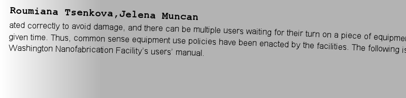
Equipment,ated correctly to avoid damage, and there can be multiple users waiting for their turn on a piece of equipment at any given time. Thus, common sense equipment use policies have been enacted by the facilities. The following is taken from Washington Nanofabrication Facility’s users’ manual.作者: Camouflage 時間: 2025-3-22 16:10
Designing for MEMS,n wafer as the build platform or machining it to be the final device. Everything discussed in this book has been used for subtractive processes, as the equipment available in the NNCI facilities is mainly designed for subtractive techniques.作者: Camouflage 時間: 2025-3-22 17:07
Imaging and Metrology, to check the quality and integrity of your devices after each process. Just remember that some process steps, like a spin coat of photoresist, are light sensitive. Some rooms have darkroom-style amber lighting, but not all, so double-check where it is safe to transport your coated wafer.作者: scrutiny 時間: 2025-3-22 23:07 作者: 極深 時間: 2025-3-23 03:40 作者: 向外才掩飾 時間: 2025-3-23 09:00 作者: critique 時間: 2025-3-23 11:16 作者: Carcinogenesis 時間: 2025-3-23 17:46
Intellectual Property,perty. Essentially, you are renting time in their facilities. As with anything, do not disclose what you do not want people to know. For those aspects you need to disclose, you need to have a nondisclosure agreement in place with the facility (if allowed).作者: 眉毛 時間: 2025-3-23 21:44
Getting Project Assistance, as independent contractors on a short- or long-term basis. These contractors do not work for the facility, but are available for private hire. This can shorten the learning curve and provide additional intellectual property isolation.作者: 圣人 時間: 2025-3-24 00:00
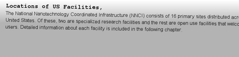
Costs,noscale science, engineering, and technology to academic, government, and industrial researchers and hands-on education and outreach events for novice users. Costs depend upon the type of user, and those are outlined in this chapter.作者: PRISE 時間: 2025-3-24 02:44 作者: Astigmatism 時間: 2025-3-24 08:35
Designing for MEMS,n wafer as the build platform or machining it to be the final device. Everything discussed in this book has been used for subtractive processes, as the equipment available in the NNCI facilities is mainly designed for subtractive techniques.作者: GROSS 時間: 2025-3-24 13:19 作者: 最低點 時間: 2025-3-24 17:32 作者: 改良 時間: 2025-3-24 19:42
Beyond NNCI: International Facilities,aboratory options with details on how to contact them for further information. This list is far from comprehensive, but is a good start for those seeking to use international MEMS fabrication facilities.作者: 冒號 時間: 2025-3-25 02:17
Intellectual Property,perty. Essentially, you are renting time in their facilities. As with anything, do not disclose what you do not want people to know. For those aspects you need to disclose, you need to have a nondisclosure agreement in place with the facility (if allowed).作者: conquer 時間: 2025-3-25 04:45 作者: cutlery 時間: 2025-3-25 10:04 作者: promote 時間: 2025-3-25 12:59
Roumiana Tsenkova,Jelena Muncanated correctly to avoid damage, and there can be multiple users waiting for their turn on a piece of equipment at any given time. Thus, common sense equipment use policies have been enacted by the facilities. The following is taken from Washington Nanofabrication Facility’s users’ manual.作者: 預(yù)防注射 時間: 2025-3-25 19:19 作者: 蹣跚 時間: 2025-3-25 20:19 作者: Acumen 時間: 2025-3-26 03:58
Overview of the Aquatic Ecosystem,regionally is the best choice, as you can be more actively involved and travel becomes more feasible. However, if you are looking for an academic collaborator, you will want to use the facility closest to them.作者: WAG 時間: 2025-3-26 08:18 作者: 食品室 時間: 2025-3-26 11:37 作者: 輕浮思想 時間: 2025-3-26 15:39
Overview of the Aquatic Ecosystem, as independent contractors on a short- or long-term basis. These contractors do not work for the facility, but are available for private hire. This can shorten the learning curve and provide additional intellectual property isolation.作者: 格子架 時間: 2025-3-26 20:40 作者: Conquest 時間: 2025-3-26 23:05
Deborah MunroIntroduces the MEMS fabrication processes and equipment.Explains how to take the first steps - where to start and get initial advice and further assistance.Includes a global list of MEMS facilities an作者: 刻苦讀書 時間: 2025-3-27 05:09 作者: APNEA 時間: 2025-3-27 05:39
Roumiana Tsenkova,Jelena MuncanMEMS devices are fabricated on silicon wafers, usually 100 mm in diameter by 600 μm thick. These fragile wafers must be handled with care, which requires use of special tools and other supplies. The details of these are outlined in the following chapter.作者: 危險 時間: 2025-3-27 12:45
James Gott,Rolf Morgenstern,Maja Turn?ekA rapidly advancing area of MEMS is the fabrication of soft materials. These polymer-, paper-, and hydrogel-based devices have unique advantages as compared to traditional hard materials like silicon. They can be very low cost and fabricated without the need for expensive capital equipment by using molding techniques and bioprinting.作者: Counteract 時間: 2025-3-27 15:19
https://doi.org/10.1007/978-981-10-0780-4Eventually, you will be done with your MEMS device, or at least be ready to transport your work to another location. The best option is always to hand carry, but that is not always feasible. These devices are small and fragile, so below is some advice on how to best prepare for shipping.作者: Anticonvulsants 時間: 2025-3-27 20:46 作者: PHON 時間: 2025-3-28 00:01 作者: EXULT 時間: 2025-3-28 05:15 作者: Credence 時間: 2025-3-28 07:31
Soft Materials and Bioprinting,A rapidly advancing area of MEMS is the fabrication of soft materials. These polymer-, paper-, and hydrogel-based devices have unique advantages as compared to traditional hard materials like silicon. They can be very low cost and fabricated without the need for expensive capital equipment by using molding techniques and bioprinting.作者: sultry 時間: 2025-3-28 14:23 作者: Orgasm 時間: 2025-3-28 18:34 作者: Obsessed 時間: 2025-3-28 19:22 作者: fatuity 時間: 2025-3-29 02:51
Ethics, Governance and Regulation in a host of electronic devices, doing tasks that were previously only conceived of in science fiction. Sensors the size of a flea can now measure strain or temperature or resistivity. They can also measure acceleration, frequency, and electrical impulses. MEMS devices are used in microscopic gears作者: eardrum 時間: 2025-3-29 03:12 作者: Infirm 時間: 2025-3-29 10:13 作者: MOAT 時間: 2025-3-29 11:41
Roumiana Tsenkova,Jelena Muncan the graphic that illustrates this basic process. You start with a silicon wafer and apply a photosensitive coating to it that is called photoresist. When you expose your coated wafer to UV light, the regions blocked by your glass mask (containing your pattern for that layer) are not exposed. Thus, 作者: accomplishment 時間: 2025-3-29 16:13 作者: 航海太平洋 時間: 2025-3-29 22:34
Aquaphotomics for Bio-diagnostics in Dairyn wafer as the build platform or machining it to be the final device. Everything discussed in this book has been used for subtractive processes, as the equipment available in the NNCI facilities is mainly designed for subtractive techniques.作者: Defiance 時間: 2025-3-30 00:10 作者: 羽毛長成 時間: 2025-3-30 06:53 作者: AWE 時間: 2025-3-30 10:03 作者: 凹室 時間: 2025-3-30 12:39
Overview of the Aquatic Ecosystem,regionally is the best choice, as you can be more actively involved and travel becomes more feasible. However, if you are looking for an academic collaborator, you will want to use the facility closest to them.作者: judiciousness 時間: 2025-3-30 18:43 作者: 憤怒歷史 時間: 2025-3-30 23:09
Introduction to Aquatic Biopolymers,perty. Essentially, you are renting time in their facilities. As with anything, do not disclose what you do not want people to know. For those aspects you need to disclose, you need to have a nondisclosure agreement in place with the facility (if allowed).作者: 火光在搖曳 時間: 2025-3-31 03:05
Overview of the Aquatic Ecosystem, as independent contractors on a short- or long-term basis. These contractors do not work for the facility, but are available for private hire. This can shorten the learning curve and provide additional intellectual property isolation.作者: 他姓手中拿著 時間: 2025-3-31 05:59 作者: Host142 時間: 2025-3-31 10:35 作者: 罐里有戒指 時間: 2025-3-31 13:43
978-3-030-33075-0Springer Nature Switzerland AG 2019作者: 頭盔 時間: 2025-3-31 18:03 作者: thyroid-hormone 時間: 2025-3-31 22:13 作者: BOOST 時間: 2025-4-1 04:57 作者: 種子 時間: 2025-4-1 07:03
Testing,miniaturize or incorporate one thing at a time until you achieve your final configuration. This will save you a lot of time and frustration in the long run. The following sections are on types of testing you may need to ensure proper performance of your MEMS device.作者: annexation 時間: 2025-4-1 10:29
Meet the Lab Directors,he lab operations on a day-to-day basis. These people are your allies, and their mission is for you to have a successful experience at their facility, so get to know them! Below are interviews with two lab directors, Dr. Michael Khbeis at the University of Washington and Dr. Jiangdong “JD” Deng at Harvard University.作者: CEDE 時間: 2025-4-1 17:35 作者: 整頓 時間: 2025-4-1 19:17
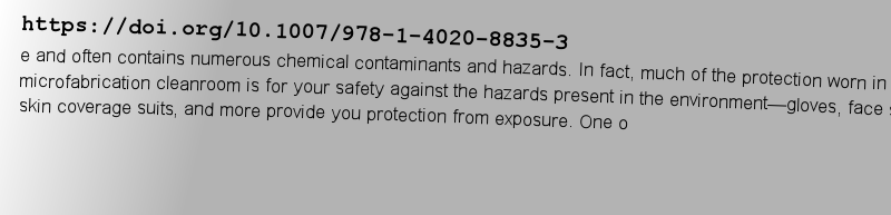
Working in a Cleanroom,f the hardest habits for many to overcome is their desire to shake hands with others while in the cleanroom. This is simply not done, as it can transfer toxic chemicals from one person to another. There are no doorknobs for the same reason.作者: 追蹤 時間: 2025-4-1 23:48
Roumiana Tsenkova,Jelena Muncanme regions are vulnerable to the etching process and get etched away. The depth and shape of the etching is dependent on the process used, the amount of time, and the crystal orientation of the wafer. When completed, the wafer is rinsed in a different solution, such as acetone, and the final result (for that layer) can be seen.