標(biāo)題: Titlebook: Cryogenic Operation of Silicon Power Devices; Ranbir Singh,B. Jayant Baliga Book 1998 Springer Science+Business Media New York 1998 Diode. [打印本頁] 作者: 令人不愉快 時間: 2025-3-21 16:33
書目名稱Cryogenic Operation of Silicon Power Devices影響因子(影響力)
書目名稱Cryogenic Operation of Silicon Power Devices影響因子(影響力)學(xué)科排名
書目名稱Cryogenic Operation of Silicon Power Devices網(wǎng)絡(luò)公開度
書目名稱Cryogenic Operation of Silicon Power Devices網(wǎng)絡(luò)公開度學(xué)科排名
書目名稱Cryogenic Operation of Silicon Power Devices被引頻次
書目名稱Cryogenic Operation of Silicon Power Devices被引頻次學(xué)科排名
書目名稱Cryogenic Operation of Silicon Power Devices年度引用
書目名稱Cryogenic Operation of Silicon Power Devices年度引用學(xué)科排名
書目名稱Cryogenic Operation of Silicon Power Devices讀者反饋
書目名稱Cryogenic Operation of Silicon Power Devices讀者反饋學(xué)科排名
作者: Original 時間: 2025-3-21 23:45 作者: –吃 時間: 2025-3-22 02:21 作者: Adj異類的 時間: 2025-3-22 06:12 作者: 奇思怪想 時間: 2025-3-22 11:56
978-1-4613-7635-4Springer Science+Business Media New York 1998作者: 我怕被刺穿 時間: 2025-3-22 16:30
Power Electronics and Power Systemshttp://image.papertrans.cn/d/image/240503.jpg作者: 我怕被刺穿 時間: 2025-3-22 20:45 作者: Cursory 時間: 2025-3-22 22:46
Beginning the Role-play Workshopon of certain key silicon properties with temperature. In silicon, a reduction in temperature has an affect on the availability of free carriers, forbidden bandgap, intrinsic carrier concentration, carrier mobilities, carrier lifetimes and impact ionization coefficients. This chapter summarizes the 作者: 暴行 時間: 2025-3-23 02:13 作者: Debark 時間: 2025-3-23 08:02 作者: 突變 時間: 2025-3-23 12:59 作者: 無畏 時間: 2025-3-23 17:35 作者: Ischemia 時間: 2025-3-23 20:45 作者: theta-waves 時間: 2025-3-23 23:03
https://doi.org/10.1007/978-981-10-7248-2r forward blocking and on-state characteristics as compared to other JFET structures. The gates in the JFET are formed by . diffusions into trenches so that more effective channel pinch off can be achieved in the forward blocking mode. To operate a JFET in the forward blocking mode, a sufficiently l作者: V洗浴 時間: 2025-3-24 06:14
Wastewater Management Through Aquacultureent between the anode and cathode terminals, a small positive bias (<1V) is applied between the gate and cathode terminals. The device then behaves like a forward biased .-i-. diode between the anode and cathode terminals. An AFCT can operate at large current densities with a relatively small forwar作者: 媽媽不開心 時間: 2025-3-24 10:18
https://doi.org/10.1007/978-981-10-7248-2 and Anode respectively, and the contact to the p-base is the Gate. A Thyristor usually operates in two distinct states in the forward direction (anode voltage positive with respect to the cathode): a low current, high voltage forward blocking state; and a high current, low voltage on-state. In the 作者: Arroyo 時間: 2025-3-24 13:09
S. Jana,Ken Gnanakan,B. B. Janamance of most of the commercial power devices used in the industry today. At cryogenic temperatures, both the performance of various devices and the applications change. In addition, most devices designed to operate in a cryogenic environment require attention on certain aspects, which may not be im作者: angiography 時間: 2025-3-24 15:52 作者: 忘恩負(fù)義的人 時間: 2025-3-24 21:29 作者: Inflammation 時間: 2025-3-25 00:13
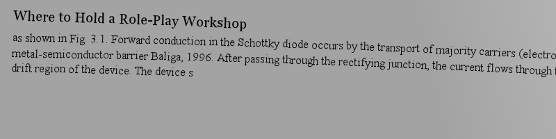
Schottky Barrier Diodes,as shown in Fig. 3.1. Forward conduction in the Schottky diode occurs by the transport of majority carriers (electrons) across the metal-semiconductor barrier Baliga, 1996. After passing through the rectifying junction, the current flows through the resistive drift region of the device. The device s作者: 破裂 時間: 2025-3-25 03:45
P-I-N Diode,ut conducts current when a positive voltage is applied to the anode. It consists of an intrinsic layer sandwiched between a pn junction. The intrinsic layer has a very low concentration of (generally) n-type in the order of 10.. It’s thickness ranges from 10μ. to 500μ. depending on the rated breakdo作者: 冒號 時間: 2025-3-25 08:09 作者: Surgeon 時間: 2025-3-25 14:44 作者: oxidize 時間: 2025-3-25 17:41 作者: Conflict 時間: 2025-3-25 22:02 作者: FILTH 時間: 2025-3-26 03:24
Asymmetric Field Controlled Thyristors,ent between the anode and cathode terminals, a small positive bias (<1V) is applied between the gate and cathode terminals. The device then behaves like a forward biased .-i-. diode between the anode and cathode terminals. An AFCT can operate at large current densities with a relatively small forwar作者: –scent 時間: 2025-3-26 07:37 作者: 雪白 時間: 2025-3-26 10:55 作者: 注意到 時間: 2025-3-26 14:59
Book 1998tures. In this case, the objective was to ob- tain higher switching speeds than are possible at ambient temperatures with the critical issue being the operating characteristics of semiconductor switches under cryogenic conditions. By 1980, cryogenic electronics was established as another branch of e作者: Blemish 時間: 2025-3-26 18:53
2196-3185 being the operating characteristics of semiconductor switches under cryogenic conditions. By 1980, cryogenic electronics was established as another branch of e978-1-4613-7635-4978-1-4615-5751-7Series ISSN 2196-3185 Series E-ISSN 2196-3193 作者: 語言學(xué) 時間: 2025-3-27 00:27 作者: CRAFT 時間: 2025-3-27 01:14
e and collector regions determine the Collector-base breakdown voltage of the device and the collector-emitter breakdown voltage is determined by the collector-base breakdown and the current gain of the transistor. While the power bipolar transistors provide a very low voltge drop to the main curren作者: outer-ear 時間: 2025-3-27 06:39
n-state, the merit of a DMOSFET is judged by the total resistance it offers to the flow of current (on-resistance) and also the rate of change of drain current with the change in gate bias (transconductance). The gate bias at which an inversion layer is formed (threshold voltage) is also an importan作者: Melodrama 時間: 2025-3-27 11:15
https://doi.org/10.1007/978-981-10-7248-2s called the maximum blocking voltage of the device. Depending on the design of the JFET, this capability may be limited by either the avalanche breakdown of the gate-source junction or the device edge termination. To switch the device from the on-state to the forward blocking state, a negative gate作者: Inclement 時間: 2025-3-27 16:10
https://doi.org/10.1007/978-981-10-7248-2responds to a reducing breakover voltage. For a rated gate trigger current, the breakover voltage can be reduced to the built-in voltage of a pn junction and thereafter, the forward characteristics resemble those of a p-i-n diode. To turn the device off from the forward on-state to a forward blockin作者: 責(zé)難 時間: 2025-3-27 20:23 作者: 施加 時間: 2025-3-27 23:13
Power Bipolar Transistors,e and collector regions determine the Collector-base breakdown voltage of the device and the collector-emitter breakdown voltage is determined by the collector-base breakdown and the current gain of the transistor. While the power bipolar transistors provide a very low voltge drop to the main curren作者: sigmoid-colon 時間: 2025-3-28 04:12 作者: muscle-fibers 時間: 2025-3-28 08:07 作者: 嗎啡 時間: 2025-3-28 10:26
Thyristors,responds to a reducing breakover voltage. For a rated gate trigger current, the breakover voltage can be reduced to the built-in voltage of a pn junction and thereafter, the forward characteristics resemble those of a p-i-n diode. To turn the device off from the forward on-state to a forward blockin作者: Albumin 時間: 2025-3-28 17:50
Temperature Dependence of Silicon Properties,idden bandgap, intrinsic carrier concentration, carrier mobilities, carrier lifetimes and impact ionization coefficients. This chapter summarizes the currently accepted models of temperature dependence of these silicon properties.作者: vector 時間: 2025-3-28 20:51
Insulated Gate Bipolar Transistors,s compared to bipolar power transistors and gate turn off thyristors. In the on-state, the emitter of an asymmetric n-channel IGBT (shown in Fig. 7.1) is grounded and a positive bias is applied at the gate to form an inversion layer in the P-base below the gate electrode.作者: 烤架 時間: 2025-3-29 02:49 作者: 打折 時間: 2025-3-29 05:57
Where to Hold a Role-Play Workshopupports a maximum reverse bias depending on the properties of the . drift region. The physical mechanisms responsible for these characteristics and their temperature dependence are explained in the following sections.作者: 沉積物 時間: 2025-3-29 09:04 作者: Saline 時間: 2025-3-29 13:10 作者: minimal 時間: 2025-3-29 18:49
Synopsis,portant at room temperature The choice of a particular device depends upon its safe operating area, breakdown voltage, the on-state voltage drop, the speed, temperature stability, packaging and gating constraints. It is essential to revise the appropriateness of devices and applications for cryogenic operation.作者: 黃瓜 時間: 2025-3-29 21:03
2196-3185 ties to a prac- tical means of fabricating electrical components and devices with lossless con- ductors. Using liquid helium as a coolant, the successful construction and operation of high field strength magnet systems, alternators, motors and trans- mission lines was announced. These developments u作者: 災(zāi)禍 時間: 2025-3-30 03:29
Beginning the Role-play Workshopidden bandgap, intrinsic carrier concentration, carrier mobilities, carrier lifetimes and impact ionization coefficients. This chapter summarizes the currently accepted models of temperature dependence of these silicon properties.作者: Blanch 時間: 2025-3-30 04:58 作者: 盲信者 時間: 2025-3-30 11:33 作者: DAMP 時間: 2025-3-30 15:20
Book 1998prac- tical means of fabricating electrical components and devices with lossless con- ductors. Using liquid helium as a coolant, the successful construction and operation of high field strength magnet systems, alternators, motors and trans- mission lines was announced. These developments ushered in