標(biāo)題: Titlebook: Bits on Chips; Harry Veendrick Book 2019Latest edition Springer International Publishing AG, part of Springer Nature 2019 Introduction to [打印本頁(yè)] 作者: osteomalacia 時(shí)間: 2025-3-21 18:50
書(shū)目名稱Bits on Chips影響因子(影響力)
書(shū)目名稱Bits on Chips影響因子(影響力)學(xué)科排名
書(shū)目名稱Bits on Chips網(wǎng)絡(luò)公開(kāi)度
書(shū)目名稱Bits on Chips網(wǎng)絡(luò)公開(kāi)度學(xué)科排名
書(shū)目名稱Bits on Chips被引頻次
書(shū)目名稱Bits on Chips被引頻次學(xué)科排名
書(shū)目名稱Bits on Chips年度引用
書(shū)目名稱Bits on Chips年度引用學(xué)科排名
書(shū)目名稱Bits on Chips讀者反饋
書(shū)目名稱Bits on Chips讀者反饋學(xué)科排名
作者: 修正案 時(shí)間: 2025-3-21 21:36
What Is a Chip?imply .. Generally the word chip refers to a small and very thin piece of material, sometimes broken from a larger piece of material. When a chip is not yet packaged, we call it a .. So, most integrated circuits are produced as dies on very thin (less than 1 mm thick) silicon wafers (Fig. 2.1). Usua作者: 敲詐 時(shí)間: 2025-3-22 02:37 作者: FACET 時(shí)間: 2025-3-22 05:43
The Chip Development Cycle steps. Because about 90% of all ICs are made in a complementary metal oxide semiconductor (.) process, this section, but also the remaining of the book, will be focussed on this technology only. For the following discussions, the reader is advised to regularly refer to the figure below.作者: 皮薩 時(shí)間: 2025-3-22 11:31 作者: grounded 時(shí)間: 2025-3-22 13:06
Analog IP, Interfaces and Integrationrest. On the contrary, the performance of the analog circuits and chip interfaces may be the differentiating factor to achieve the best overall system performance. A short summary on these circuits is therefore a minimum requirement to complete the picture of integrated circuits.作者: ILEUM 時(shí)間: 2025-3-22 20:31
Wafers and Transistors a very dominant role in their performance and reliability. Aware of this fact, Lilienfeld used copper sulphide as a semiconductor starting material in 1930. Germanium was used during the early 1950s. Until 1960, however, usable . could not be manufactured. During the 1960s, the move from germanium 作者: OCTO 時(shí)間: 2025-3-22 23:16
Lithographyns in all layers are represented in a layout. The generation of such a layout is usually done via an interactive graphics display for handcrafted layouts (certain analog circuits and/or some basic digital cells) or by means of synthesis, place-and-route and floor-planning tools, as discussed in Chap作者: GROSS 時(shí)間: 2025-3-23 02:26
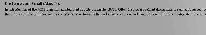
Fabricationhe introduction of the MOS transistor in integrated circuits during the 1970s. Often the process-related discussions are either focussed towards that part of the process in which the transistors are fabricated or towards the part in which the contacts and interconnections are fabricated. These parts作者: 不愛(ài)防注射 時(shí)間: 2025-3-23 06:43 作者: Externalize 時(shí)間: 2025-3-23 13:33
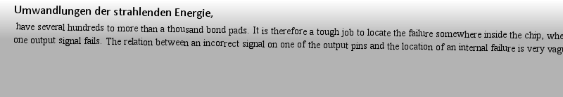
Failure Analysis have several hundreds to more than a thousand bond pads. It is therefore a tough job to locate the failure somewhere inside the chip, when, for instance, one output signal fails. The relation between an incorrect signal on one of the output pins and the location of an internal failure is very vague作者: Valves 時(shí)間: 2025-3-23 17:09 作者: 光明正大 時(shí)間: 2025-3-23 21:31 作者: 肥料 時(shí)間: 2025-3-23 22:27
Desinfektion und Chemotherapie,ot yet packaged, we call it a .. So, most integrated circuits are produced as dies on very thin (less than 1 mm thick) silicon wafers (Fig. 2.1). Usually 25 or 50 wafers are produced in one . or .. Specialists would immediately recognise the conventional 6 inch wafer, but the figure perfectly illustrates the different phases of a chip.作者: Crepitus 時(shí)間: 2025-3-24 05:43 作者: notion 時(shí)間: 2025-3-24 07:05 作者: 冷漠 時(shí)間: 2025-3-24 10:53
What Is a Chip?ot yet packaged, we call it a .. So, most integrated circuits are produced as dies on very thin (less than 1 mm thick) silicon wafers (Fig. 2.1). Usually 25 or 50 wafers are produced in one . or .. Specialists would immediately recognise the conventional 6 inch wafer, but the figure perfectly illustrates the different phases of a chip.作者: 強(qiáng)制性 時(shí)間: 2025-3-24 17:33
Digital Circuits and IP because of its importance. Basically, a MOS transistor has three terminals: a gate, a source and a drain (Fig. 5.1). The gate is separated from the channel region by only an extremely thin (..) insulating gate oxide.作者: HPA533 時(shí)間: 2025-3-24 20:07 作者: Benign 時(shí)間: 2025-3-25 01:18
,Spektroskopie der R?ntgenstrahlen,cus of the ITRS towards seven topics and continued with an ITRS 2.0 version. With the end of Moore’s Law at the horizon, ITRS 2016 has become the final roadmap and will be replaced by a new initiative, named the . (.), which now also include . or . devices.作者: 思鄉(xiāng)病 時(shí)間: 2025-3-25 03:44
And, What Is Next?cus of the ITRS towards seven topics and continued with an ITRS 2.0 version. With the end of Moore’s Law at the horizon, ITRS 2016 has become the final roadmap and will be replaced by a new initiative, named the . (.), which now also include . or . devices.作者: HALO 時(shí)間: 2025-3-25 09:42 作者: 用不完 時(shí)間: 2025-3-25 14:46
Umwandlungen der strahlenden Energie,wever, this is not enough. Logical (design) errors are relatively easy to detect and to locate during scan test and in full functional test. The cause of timing errors, e.g. due to the occurrence of noise, can be so complex that even with the most advanced failure analysis techniques, it can take months before the correct diagnosis can be made.作者: slow-wave-sleep 時(shí)間: 2025-3-25 18:50 作者: 分解 時(shí)間: 2025-3-25 22:51
Book 2019Latest editiond to be accessible to readers with limited, technical knowledge and coverage includes key aspects of integrated circuit design, implementation, fabrication and application. The author complements his discussion with a large number of diagrams and photographs, in order to reinforce the explanations. 作者: 立即 時(shí)間: 2025-3-26 03:56 作者: 冷淡周邊 時(shí)間: 2025-3-26 07:45 作者: 軍械庫(kù) 時(shí)間: 2025-3-26 12:08
https://doi.org/10.1007/978-3-662-41631-0 V/μm, which is much more than the maximum breakdown field in germanium but still less than that in silicon. Another reason is the widely accepted military spec, which can be met with this material. This spec requires products to function correctly at a maximum operating temperature of 125 °C. The m作者: cuticle 時(shí)間: 2025-3-26 16:16
The Electronics (R)evolutionnnected. These interconnected components implement specific functions which are each tailored to a target application. The semiconductor material is usually silicon, but alternatives include germanium and gallium arsenide.作者: orthopedist 時(shí)間: 2025-3-26 19:31 作者: Expressly 時(shí)間: 2025-3-26 21:39
The Chip Development Cycle steps. Because about 90% of all ICs are made in a complementary metal oxide semiconductor (.) process, this section, but also the remaining of the book, will be focussed on this technology only. For the following discussions, the reader is advised to regularly refer to the figure below.作者: 平項(xiàng)山 時(shí)間: 2025-3-27 02:02 作者: anaerobic 時(shí)間: 2025-3-27 05:30 作者: DECRY 時(shí)間: 2025-3-27 10:04 作者: 束縛 時(shí)間: 2025-3-27 15:03 作者: mortuary 時(shí)間: 2025-3-27 21:21 作者: enlist 時(shí)間: 2025-3-28 00:24
Desinfektion und Chemotherapie, steps. Because about 90% of all ICs are made in a complementary metal oxide semiconductor (.) process, this section, but also the remaining of the book, will be focussed on this technology only. For the following discussions, the reader is advised to regularly refer to the figure below.作者: apropos 時(shí)間: 2025-3-28 02:18
Peripheres Nervensystem. Lokalan?sthesierest. On the contrary, the performance of the analog circuits and chip interfaces may be the differentiating factor to achieve the best overall system performance. A short summary on these circuits is therefore a minimum requirement to complete the picture of integrated circuits.作者: 牽索 時(shí)間: 2025-3-28 06:44
Die Lehre vom Schall (Akustik),he introduction of the MOS transistor in integrated circuits during the 1970s. Often the process-related discussions are either focussed towards that part of the process in which the transistors are fabricated or towards the part in which the contacts and interconnections are fabricated. These parts are called . and ., respectively.作者: 相符 時(shí)間: 2025-3-28 13:57
Die Lehre vom Schall (Akustik),only those applications that really required the low-power features of CMOS were designed in it. Most examples, then, were battery-supplied applications, such as wristwatches, pocket calculators, portable medical devices (hearing aids and implantable heart controls) and remote controls.作者: BOLUS 時(shí)間: 2025-3-28 18:18
Desinfektion und Chemotherapie,nnected. These interconnected components implement specific functions which are each tailored to a target application. The semiconductor material is usually silicon, but alternatives include germanium and gallium arsenide.作者: sclera 時(shí)間: 2025-3-28 19:50
Desinfektion und Chemotherapie,imply .. Generally the word chip refers to a small and very thin piece of material, sometimes broken from a larger piece of material. When a chip is not yet packaged, we call it a .. So, most integrated circuits are produced as dies on very thin (less than 1 mm thick) silicon wafers (Fig. 2.1). Usua作者: 滑稽 時(shí)間: 2025-3-29 00:32 作者: 不在灌木叢中 時(shí)間: 2025-3-29 04:31 作者: filicide 時(shí)間: 2025-3-29 07:27
https://doi.org/10.1007/978-3-662-37850-2OS and a pMOS transistor. As the MOS transistor is the basic element of 90% of all integrated circuits, we will repeat some of the material in Part I, because of its importance. Basically, a MOS transistor has three terminals: a gate, a source and a drain (Fig. 5.1). The gate is separated from the c作者: 束縛 時(shí)間: 2025-3-29 15:07 作者: vasospasm 時(shí)間: 2025-3-29 18:14
https://doi.org/10.1007/978-3-662-41631-0 a very dominant role in their performance and reliability. Aware of this fact, Lilienfeld used copper sulphide as a semiconductor starting material in 1930. Germanium was used during the early 1950s. Until 1960, however, usable . could not be manufactured. During the 1960s, the move from germanium 作者: committed 時(shí)間: 2025-3-29 20:12
Zentralnervensystem (Narkose und Verwandtes)ns in all layers are represented in a layout. The generation of such a layout is usually done via an interactive graphics display for handcrafted layouts (certain analog circuits and/or some basic digital cells) or by means of synthesis, place-and-route and floor-planning tools, as discussed in Chap作者: 不能平靜 時(shí)間: 2025-3-30 01:52 作者: 事物的方面 時(shí)間: 2025-3-30 07:09
Die Lehre vom Schall (Akustik),only those applications that really required the low-power features of CMOS were designed in it. Most examples, then, were battery-supplied applications, such as wristwatches, pocket calculators, portable medical devices (hearing aids and implantable heart controls) and remote controls.作者: 暴露他抗議 時(shí)間: 2025-3-30 09:38 作者: Champion 時(shí)間: 2025-3-30 15:01 作者: alcohol-abuse 時(shí)間: 2025-3-30 17:02
https://doi.org/10.1007/978-3-319-76096-4Introduction to integrated circuits; Microelectronics basics; Semiconductor basics; Microchip basics; CM作者: 可能性 時(shí)間: 2025-3-30 21:33 作者: paroxysm 時(shí)間: 2025-3-31 04:19 作者: 真 時(shí)間: 2025-3-31 05:31 作者: oracle 時(shí)間: 2025-3-31 12:43 作者: FACET 時(shí)間: 2025-3-31 13:49