標(biāo)題: Titlebook: Alternative Lithography; Unleashing the Poten Clivia M. Sotomayor Torres Book 2003 Springer Science+Business Media New York 2003 electronic [打印本頁] 作者: 母牛膽小鬼 時間: 2025-3-21 17:05
書目名稱Alternative Lithography影響因子(影響力)
作者: 河潭 時間: 2025-3-21 22:38 作者: 聽覺 時間: 2025-3-22 02:19
3 Diamagnetic susceptibility of AlH4NO8S2,teresting observation is that in most of the works reported so far (except the early works in ref. 2,3 above) the feature sizes have rather been closer to the 100 nm domain than to the 10 nm domain. Furthermore in most of the NIL experiments reported the de-scribed were made with stamps having areas作者: CRUDE 時間: 2025-3-22 06:43
https://doi.org/10.1007/978-3-540-44736-8 This mature technique combines high resolution (<10 nm),. dimensional control, alignment capability and high nano-magnetism and turned out to be the technique of choice for nanopatterning. However, despite the progress on electron beam resist sensitivity and low voltage EBL, this technique due to i作者: 神經(jīng) 時間: 2025-3-22 08:45
https://doi.org/10.1007/978-3-540-44736-8 known methods of inducing molecules to self-assemble onto a surface from the liquid or vapor phase, they discovered that self-assembly can also occur when a polymeric membrane impregnated with the same kind of molecules is brought into contact with a convenient substrate. The membrane, acting as a 作者: 無瑕疵 時間: 2025-3-22 16:42 作者: Amenable 時間: 2025-3-22 20:53 作者: 下級 時間: 2025-3-22 23:20
Alternative Lithography,fe sciences. Alternative techniques to cost-intensive or limited-access fabrication methods with nanometre resolution have been under biologi-cal for nearly two decades. One clear example is the evolving set of scanning probes techniques, which has become ubiquitous in many research areas. If one co作者: 針葉 時間: 2025-3-23 01:26
Viscoelastic Properties of Polymers,cess have been developed, which are reviewed in considerable detail. . Most of them share a common principle: a pattern is transferred into a fluid layer by embossing the mould into it. Usually a thin polymer layer spun on a silicon substrate is moulded by a sequence of steps, which are schematicall作者: hardheaded 時間: 2025-3-23 05:53
Wafer Scale Nanoimprint Lithography,teresting observation is that in most of the works reported so far (except the early works in ref. 2,3 above) the feature sizes have rather been closer to the 100 nm domain than to the 10 nm domain. Furthermore in most of the NIL experiments reported the de-scribed were made with stamps having areas作者: inferno 時間: 2025-3-23 11:58 作者: multiply 時間: 2025-3-23 17:49 作者: 口音在加重 時間: 2025-3-23 19:23 作者: investigate 時間: 2025-3-23 23:13
1571-5744 r, that there was no point to investigate only alternative devices to CMOS, but what was really needed was an integrated approach that took into account more fa978-1-4613-4836-8978-1-4419-9204-8Series ISSN 1571-5744 Series E-ISSN 2197-7976 作者: Classify 時間: 2025-3-24 05:11 作者: CHIP 時間: 2025-3-24 06:45
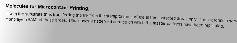
https://doi.org/10.1007/978-3-540-44736-8ct with the substrate thus transferring the ink from the stamp to the surface at the contacted areas only. The ink forms a self-assembled monolayer (SAM) at these areas. This leaves a patterned surface on which the master patterns have been replicated.作者: Nonconformist 時間: 2025-3-24 14:21
https://doi.org/10.1007/978-3-540-44736-8s are suitable for the development of a scanning probe-based lithography. Ultra high vacuum requirements, low temperatures or unreliable pattern definition mod-ification considerably the number of methods suitable for lithographic purposes. In this context lithography means a method for large scale patterning of surfaces and device fabrication.作者: abject 時間: 2025-3-24 15:18
https://doi.org/10.1007/978-3-540-44736-8Roadmap for Semiconductors (ITRS) sub 100 nm patterning is a great demand for next generation lithography (NGL). Advanced technologies, such as extreme ultraviolet lithography (EUV), X-ray lithography (XRL), electron projection lithography (EPL), and ion projection lithography (IPL) are pushing towards into the domain of 35 nm..作者: 易改變 時間: 2025-3-24 20:24 作者: nonchalance 時間: 2025-3-25 02:29 作者: grovel 時間: 2025-3-25 05:46
Local Oxidation Nanolithography,s are suitable for the development of a scanning probe-based lithography. Ultra high vacuum requirements, low temperatures or unreliable pattern definition mod-ification considerably the number of methods suitable for lithographic purposes. In this context lithography means a method for large scale patterning of surfaces and device fabrication.作者: Pseudoephedrine 時間: 2025-3-25 09:55 作者: entail 時間: 2025-3-25 14:02
Nanoimprint Lithography,oday is that we still do not have a mature nanostructure manufacturing technology that has the needed low-cost and high-throughput. Nanoimprint lithography is one of the most promising low-cost, high-throughput technologies for manufacturing nanostructures. Significant developments have been made in recent years.作者: Accrue 時間: 2025-3-25 19:02
1571-5744 e and thus today ‘s wealth, would have been a source of inspiration five hundred years later. Now, it seems intuitive that a simple way to produce a large number of replicates is using a mold to emboss pattern you need, but at the nanoscale nothing is simple: the devil is in the detail. And this boo作者: Indent 時間: 2025-3-25 21:48 作者: 者變 時間: 2025-3-26 03:54
https://doi.org/10.1007/978-3-540-44736-8dwidth not remotely rivalled by terrestrial or satellite radio connections. The classical optical materials were glasses and transparent crystals. The high refractive indexes that most of these materials posses in comparison to polymers are bought for high weight and more extreme process parameters.作者: 出沒 時間: 2025-3-26 08:06 作者: 裂隙 時間: 2025-3-26 10:10 作者: semiskilled 時間: 2025-3-26 16:33 作者: 平 時間: 2025-3-26 19:11 作者: 挑剔小責(zé) 時間: 2025-3-26 22:01
Application of Nanoimprint Lithography in Magnetism,arge area patterning.. while interference lithography is a simple technique, it is only suitable for the fabrication of regular pattern arrays. Finally, ion irradiation with a stencil mask provides an interesting alternative but still considerable efforts have to be made in order to show a performance of both high resolution and high throughput.作者: HAIRY 時間: 2025-3-27 02:02
Book 2003 today ‘s wealth, would have been a source of inspiration five hundred years later. Now, it seems intuitive that a simple way to produce a large number of replicates is using a mold to emboss pattern you need, but at the nanoscale nothing is simple: the devil is in the detail. And this book is about作者: 壓迫 時間: 2025-3-27 06:54
Alternative Lithography,sometimes in the atomic scale. Depending on application, there are varying degrees of strong specifications, which have to be met in industrially relevant processes due to manufacturability and costs considerations as, for example, in the electronics industry. However, it appears that less demanding作者: 雄偉 時間: 2025-3-27 10:37
Nanoimprint Lithography,han a fundamental physical length scale, conventional theory may no longer apply and new phenomena emerge. To fully benefit from the discovery and innovation in nanostructures and commercialize them, a low-cost and high-throughput manufacturing of nanostructures is essential. One biggest challenge t作者: 禁止 時間: 2025-3-27 15:32
Viscoelastic Properties of Polymers,ts simplicity. This lithog-raphy already apparent in the works of S. Chou, .–. who demonstrated that features of a few ten’s of nanometers can be imprinted with a standard laboratory press. The lithog-raphy of embossing reach back into history and are applied today in the production of numerous prod作者: beta-cells 時間: 2025-3-27 18:51
Nanorheology,al. The viscous molding material is shaped by either pressing the hard stamp into it (embossing or imprinting) or by filling of a cavity containing a structured mold insert (casting or injection molding). In order to achieve a reasonable process time and yield, this is usually carried out under pres作者: rods366 時間: 2025-3-27 22:21
Wafer Scale Nanoimprint Lithography,gy. It got even larger attention when it was reported that sub 10 nm features on a Si stamp could be replicated into a resist layer, which in turn had a profile allowing a lift-off process to be possible..,. More reports about NIL technology followed and soon also devices were reported made with NIL作者: 藥物 時間: 2025-3-28 04:26
Step and Stamp Imprint Lithography, the semiconductor industry has relied on optical lithography and new generations of optical steppers are being developed for shorter wavelengths. Anyhow, in order to produce sub-50 nm lithography researches have started to look for new solutions, such as X-ray lithography, fast electron beam (e-bea作者: 必死 時間: 2025-3-28 09:48
Step and Flash Imprint Lithography,ools? A combination of improvements in optics, reduction in wavelength, and the introduction of more complex photomasks and processes has enabled printing of features smaller than 100 nm. These improvements came at a cost, however, and this cost has followed an exponentially in-creasing trend (1). T作者: Jejune 時間: 2025-3-28 12:18
Using PDMS as a thermocurable resist for a mold assisted imprint process,, low cost and high throughput is becoming a prime necessity. Nowadays, this demand arises not only from the microelectronics community where miniaturization has been a driving strategy since a long time, but originates from many fields: optics, photonics, nanoelectronics, nano-magnetism, nano-elect作者: encyclopedia 時間: 2025-3-28 15:08 作者: Suppository 時間: 2025-3-28 20:54
Microcontact Printing Techniques,i.e. to arrange spontaneously, as a dense, ordered and stable monolayer on suitable surfaces. Generally, these molecules contain a chemically reactive head that anchors onto the surface, and a linear flexible chain of methyl groups which orients itself approximately with the normal to the surface as作者: Incorruptible 時間: 2025-3-29 02:38 作者: 貪婪地吃 時間: 2025-3-29 03:13
Combined Approaches for Nanoelectronic Device Fabrication,lithographic resolution. For lithographic mask production and patterning of features down to a few performance, electron beam lithography (EBL) is a well established technique. Transferring the mask pattern into resist on an industrial high throughput level is mainly the domain of optical lithograph作者: ARIA 時間: 2025-3-29 09:35 作者: 類似思想 時間: 2025-3-29 14:18 作者: Painstaking 時間: 2025-3-29 19:11
Optical Applications of Nanoimprint Lithography,lasses but includes modern measurement and control systems in, for example, cars. Optical fibres have taken over information technology with their bandwidth not remotely rivalled by terrestrial or satellite radio connections. The classical optical materials were glasses and transparent crystals. The作者: 可互換 時間: 2025-3-29 19:54
Biotechnology Applications of NIL,e formed at a low cost. The real massive exploration of nanotechnology in biotechnological applications has not been hindered by lack of ideas of what to do but more about how to get it done at a sufficiently low cost. Biotechnology has for many years taken up technologies from microelectronics when作者: monopoly 時間: 2025-3-30 02:27 作者: 建筑師 時間: 2025-3-30 04:06
Nanostructure Science and Technologyhttp://image.papertrans.cn/a/image/154084.jpg作者: 希望 時間: 2025-3-30 09:52 作者: paltry 時間: 2025-3-30 13:22 作者: Dappled 時間: 2025-3-30 17:31 作者: painkillers 時間: 2025-3-30 20:43 作者: 演繹 時間: 2025-3-31 01:27
3 Diamagnetic susceptibility of AlH4NO8S2,gy. It got even larger attention when it was reported that sub 10 nm features on a Si stamp could be replicated into a resist layer, which in turn had a profile allowing a lift-off process to be possible..,. More reports about NIL technology followed and soon also devices were reported made with NIL作者: Obsessed 時間: 2025-3-31 05:17
2 Diamagnetic susceptibility of AlF3, the semiconductor industry has relied on optical lithography and new generations of optical steppers are being developed for shorter wavelengths. Anyhow, in order to produce sub-50 nm lithography researches have started to look for new solutions, such as X-ray lithography, fast electron beam (e-bea作者: Omniscient 時間: 2025-3-31 10:43 作者: 使虛弱 時間: 2025-3-31 16:37
https://doi.org/10.1007/978-3-540-44736-8, low cost and high throughput is becoming a prime necessity. Nowadays, this demand arises not only from the microelectronics community where miniaturization has been a driving strategy since a long time, but originates from many fields: optics, photonics, nanoelectronics, nano-magnetism, nano-elect作者: 同謀 時間: 2025-3-31 19:51
https://doi.org/10.1007/978-3-540-44736-8 shows the general princi-ples of μCP First, an elastomeric stamp is prepared from an already existing patterned surface, called the master, by covering the surface with a liquid prepolymer (usually poly(dimethylsiloxane), PDMS) followed by curing. The hardened elastomeric stamp is peeled off the ma作者: Glutinous 時間: 2025-3-31 22:24
https://doi.org/10.1007/978-3-540-44736-8i.e. to arrange spontaneously, as a dense, ordered and stable monolayer on suitable surfaces. Generally, these molecules contain a chemically reactive head that anchors onto the surface, and a linear flexible chain of methyl groups which orients itself approximately with the normal to the surface as作者: 虛假 時間: 2025-4-1 03:53 作者: corpus-callosum 時間: 2025-4-1 08:31
https://doi.org/10.1007/978-3-540-44736-8lithographic resolution. For lithographic mask production and patterning of features down to a few performance, electron beam lithography (EBL) is a well established technique. Transferring the mask pattern into resist on an industrial high throughput level is mainly the domain of optical lithograph